
by Carlota Figueroa
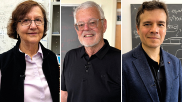
Very recently, on June 10th of this year, Eva Andrei, Pablo Jarillo-Herrero and Allan H. MacDonald were awarded the 2026 Kavli Prize in the category of Nanoscience for their foundational work establishing the field of Twistronics. I know that sounds like something straight out of a sci-fi movie, but it is one of the most pivotal (and real) discoveries that is transforming Materials Science as we know it. Let this column serve as a short (and very qualitative, as the intention is that the article is readable and enjoyable, not dense and technical) introduction to the world of quantum 2D materials. I hope that by the time you finish reading, you are as excited about the potential of this field as I am – even if this is your first time ever hearing about bilayer graphene.
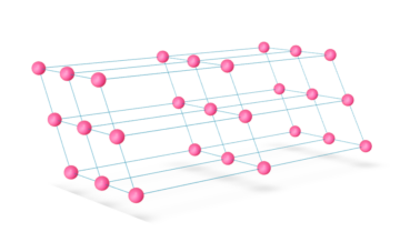
Let us start at the beginning: we must first understand what a crystalline solid is. Many of our day-to-day solids are crystalline structures: table salt, sugar, diamond and copper, just to name a few. What this means is that the atoms that make up these structures are arranged in a highly ordered microscopic structure. Imagine you could zoom into a grain of salt until you see each individual sodium and chlorine atom: you’d see they are very neatly organised in a periodic manner, so that no matter what part you zoom into, you’d see the exact same repeating pattern of sodium and chlorine atoms over and over. This periodicity and order is what characterises crystalline solids. These structures can be one-dimensional (meaning you have a chain of atoms that extends in just one dimension of space, like the x-axis), two-dimensional (so you have a sheet of atoms that extends throughout two dimensions of space, like the x- and y- axes) or three-dimensional (which is what many of us think of when we imagine a solid: some arrangement of atoms that extends along the x- y- and z- axes). We will focus on the second type: 2D crystalline structures – or solids made up of a single layer of atoms.
The discovery of stable 2D materials was in itself groundbreaking. Not very long ago, the possibility of creating an entire family of materials that was only one atom thick was unimaginable. In 2010, Andre Geim and Konstantin Novoselov received the Nobel Prize in Physics for their work on graphene. And you may ask: what even is graphene? Well, you know the normal HB and B pencils that we use to write or take our SATs? The lead in these pencils is mainly graphite (with some clay and wax to ensure they are functional), which is an allotrope of carbon: the carbon atoms are bunched up together in hexagonal layers, which describes the periodicity of the atoms on each sheet. The higher the concentration of graphite, the darker a pencil will write. This is why B pencils leave darker marks and feel softer on paper than H pencils – because they proportionally have more graphite. We can now think of graphene as a sheet of graphite that is just one atom thick. In fact, our Nobel Prize winners first produced graphene by repeatedly sticking adhesive tape (yes, the kind you can buy at any department store) on a big block of graphite, peeling off thinner and thinner flakes, and then transferring them onto a silicon wafer. Really, it’s that simple. If you are bored and want to feel like a Nobel winner, you can always grab some tape and some pencils and extract your very own sample of graphene at home (although I must warn you that it will not be a pure sample since there is some contamination from the clay and wax, but it is definitely good enough for us).
In recent years, much of the research in the field of Nanomaterials has focused on what happens when you start stacking layers of 2D materials on top of each other. More specifically, many have dedicated themselves to investigating what happens if you stack layers of graphite on top of each other and combine them with layers of other 2D materials. For some time, that is what our favourite researchers on 2D materials did: a bit like building a Lego tower, they began developing a whole new range of materials from these one-atom-thick sheets. They discovered that depending on the order in which you combined the layers, you could develop materials with practically any properties you wanted: from thermal insulators to ferromagnetic superconductors.
Nonetheless, for Eva, Pablo, and Allan, just stacking layers on top of each other wasn’t enough. They began developing the theoretical and experimental framework for Twistronics by asking: “what if we also slightly twist the layers with respect to each other?” They soon discovered that by changing the relative angle between layers, you could completely change the properties of the material you created. In fact, they even discovered the existence of a magic angle for bilayer graphene: when you twist one of the graphene layers about 1.1º with respect to the other and the last electronic band is half-filled, the material acts as an insulator, but when you slightly change the electron density, it suddenly becomes a superconductor.
To properly understand what is going on, we need to break down the previous sentence. I will not get into all of the details of how electron band theory is constructed (although, if you have some background in quantum physics, I highly recommend you check it out because it is fascinating) but I will give you all the basics – or at least try to. Think back to your high-school Physics and Chemistry classes. Our atoms are made up of a nucleus and some electrons around it. Well, in Solid-State Physics, we use these components to divide the study of our system: we consider on one hand the nucleus and the electrons on the innermost shells as a sort of massive and immovable cell that interacts with the rest of the solid via a potential. On the other hand, we have the electrons on the outermost shells, which can move throughout the solid (well, this isn’t so simple but we will let it go) and have a much smaller mass. Electronic band theory describes the different energy levels which electrons can have, which are then divided into bands. The energy of an electron can depend on many factors, like its quantum numbers (including spin, orbital type and orientation), its radial distance from the nucleus or its interaction with other electrons. At this point I need to introduce one of the most important principles in Quantum Physics: Pauli’s Exclusion Principle, which asserts that two fermions (particles with spin 1/2) cannot have the same quantum state. Our electrons are fermions! A discussion of what spin really is merits its own article but for now you just need to keep in mind that we cannot have two electrons with the exact same energy and the exact same quantum numbers. An electron has two possible spin orientations, and depending on the energy shell it occupies, it can have a range of values for orbital angular momentum and its orientation. So really, there’s a lot of possible combinations.
We can condense this into an executive (and far more useful, at least to us) summary: all of the electrons that should have the exact same energy end up having slightly different energies because they all need to have different quantum numbers. The spacing between these energy levels is so small that we group them into a band and consider it as a whole. It’s hard to think of an analogy for this, but imagine you are the CEO of a company and you have a bunch of workers that should all, in principle, earn the same monthly salary. Now imagine that these workers are all essentially the same, except they cannot be exactly the same, but these differences don’t really affect their ability to perform. Maybe one has blue eyes, maybe another has perfectly straight teeth (these are our workers’ “quantum numbers”!): all characteristics that make them slightly different from each other but still allow them to perform the exact same tasks with the same efficiency and level of outcome. For some reason, as the almighty CEO, you favour the blue-eyed worker or the worker with a great smile, so you pay them slightly more than the others. However, since these subtleties don’t affect their performance, you can’t really justify paying them an entirely different salary either, so the difference is just 10 or 20 dollars a month, enough for a couple of extra coffees during their lunch break. Hence, you now have a bunch of workers that all earn slightly different salaries but are, in the grand scheme of things, so similar, that you can group them all within the same salary range.
Now you (hopefully) understand what an electronic band is. Each electronic band has a number of allowed states, meaning that there is a limited number of electrons that can occupy each band (or a limited number of employees in each salary range), but we also have a given number of electrons in a solid (or a set number of employees in a company). They order themselves in the bands, filling up the lowest energy bands first and moving upwards. The last electronic band is half-filled when exactly half of the available positions for that energy band have been occupied by electrons.
Thanks to our decision to twist the layer of graphene, we induce interference between the layers, which results in the last electronic band being nearly flat. Why does this matter? This band shape (which describes the relationship between energy and momentum) is what forces our electrons to effectively become very “heavy” (I put this in quotation marks because the real mass of the electron doesn’t change, it is its effective mass that changes but I won’t go deeper into this) and very slow. The critical point is that their kinetic energy becomes much less important than the Coulomb energy arising from interactions with other electrons. Remember, since they are both negative charge carriers, there is a repulsive Coulomb force that appears between them. It’s similar to how two North poles on a magnet will repel each other. Normally, electrons can be treated as independent particles so that each electron’s movement can be studied on its own, without having to account for how its behaviour is altered by the presence of other electrons. However, we can only carry out this analysis because its kinetic energy is much larger than the Coulomb energy from the electrostatic interactions. But once you take away that kinetic dominance, once they stop moving very fast, the interactions between electrons become incredibly important: our electrons can no longer be treated as independent particles. This is the reason why we end up with an insulator: the electrons no longer have enough kinetic energy to overcome the repulsion with other electrons and they end up being stuck in place to balance the Coulomb interactions. Since they can no longer move, they can no longer carry their charge throughout the solid, so the material becomes unable to conduct electricity.
Let us recap. We now have two layers of graphene sitting on top of each other, with one of them slightly twisted with respect to the other, and this concoction acts as an insulating material. But this is not what we wanted: we wanted to have something that conducts electricity very well, not something that doesn’t conduct anything at all. So we change the electronic density. How? By applying a special type of potential via an external circuit. Return to the beginning of this discussion: we started off with a system where the last electronic band was exactly half full. Well, all the positions not filled by electrons are called holes, and we can treat them as positive charge carriers. Beware! These are not actually particles, but we can qualitatively treat them as such: rather than having the presence of something that carries positive charge, we have the absence of something that carries negative charge, and these two concepts can be used interchangeably. Depending on the potential we apply, we can either add more electrons to that last band or add holes, breaking the symmetry between electron and hole densities: the extra mobile carriers are the ones that will conduct electricity. When we move slightly away from that half-filling, we see that the bilayer graphene moves into a superconducting state, which means that the extra carriers we added can now conduct electricity with no resistance. In reality, superconducting states are characterised by more properties, like the ability to completely expel an external magnetic field and the formation of Cooper pairs, but when you talk about a “superconductor” the first thing that many people think of is “a perfect conductor”. And that is essentially what it is: I think delving deeper into the principles of superconductivity will make us lose focus, and honestly there is enough to say about superconductors that I could write an entire article just on these fascinating materials.
So by now you understand how bilayer graphene can be transformed from an insulator into a superconductor. Great, but why should you care? The fact that we can change a material so easily from something that does not let any electricity through to something that lets electricity through at zero resistance, with no friction, has huge industry potential. You have tunable electronics that can revolutionise switches, sensors and detector systems. You have flexible and transparent (yes, graphene is so thin that it is basically transparent to visible light) electronics, which have huge applications to wearable electronics, electrodes or touch sensors. On top of this, if superconducting bilayer graphene becomes a reliable material, it can be used to improve the superconducting circuits in quantum computers. Yes, those that the news often refers to as the “future of computing” and my dad often refers to as “a computer you can speak to that can do anything you imagine, like in Star Trek”. The sad news is that this superconductive state can only be achieved below a critical temperature: and that critical temperature is around 1.7 K (or -456.61 ºF for my American friends, and -271.45 ºC for my friends everywhere else in the world). In plain English, that’s very, very cold – cold enough that it cannot be easily used for commercial applications yet. So we still have a lot of research left to do. The good news is that the progress that has been made to date is astonishing and the potential that our researchers have is astounding: Eva, Pablo, Allan and the rest of scientists working on Twistronics are making materials that sound like they come from a sci-fi movie into a tangible reality.
***
Enjoying the content on 3QD? Help keep us going by donating now.